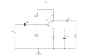
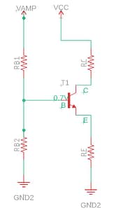
Here is the common emitter amplifier circuit. The components are generic for now. VIN supplies a small current to the base and VCC provides a larger voltage and current to the collector and load. The emitter is common to the base and collector, so the name Common Emitter. If VIN is a sine wave AC, the output will be a inverted sine wave offset by 180 degrees and amplified. High power gain with common emitter amplifier.
Capacitors:
C3 allows the AC signal to bypass RE. Increases the gain of the amplifier.
C1 and C2 blocks DC (VCC) signal and allow AC signal to passthrough
Resistor:
RB1 and RB2 are a voltage divider.
RC is the resistor on the collector
RE is the resistor on the emitter
Example:
Vin: 10mV @ 1mA
Vout (RL): 400mV @ 15mA
Gain:
AV = Vout / Vin: 400m/10mV = 40
Ai = Iout / Iin: 15mA / 1mA = 15
PIn = 10mV * 1mA = 0.01mW
POut = 400mV*15mA = 6mW
Power Gain: POut / PIn = 6mW/0.01mW = 600 = AV * AI
This is solved with voltage into base set to 0. This is the quiescent voltage.
β =100 is what most set it to. It is a safe number.
RB1 and RB2 is the biased part of the circuit. The Transistor, RC, and RE are the amplifier part. Capacitor is for input and output stages.
Resistors power limit is 0.25W. We will set PowerRC = 0.2W, you can use this for all resistors based on the spec sheet.
We se Vbias = VRE(Q) + VCB(Q) = 1.2V + 0.7V = 1.9V
to VRE(Q) to 10% of VAMP. 10% is just a rule that some use.
The base voltage is 0.7V. It is the most common setting for a transistor. RE setting will offset 0.7V being lower.
We will look at setting the voltage for the emitter side: VRE = 10% of Vamp = 12V @ 10% = 1.2V. Vbias = VRE(Q) + VCB(Q) = 1.2V + 0.7V = 1.9V
We will look at the calculations for the collector side with this: Set quiescent voltage of VRC to (12V – 1.9V) /2 = 5.05V.. You set this number to the half way point based on left over voltage from the base and emitter.
PowerRC = V * I
0.2W = 5.05V * I
IRC = 0.0396A or 39.6mA
VRC = I * R
5.05V = 39.6mA * R
RC = 127.5Ω. You can always select your RC and then calculate the power.
β * IB(Q) = IC(Q) =
IB(Q) = 39.6mA / 100 = 0.396mA = 0.000396A
IE = IB + IC
=39.6mA + 0.396mA = 39.996mA or 40mA
RE = VE / IE = 1.2V / 0.040 = 30Ω
Now we look at the other side of the circuit the biased side with resistors RB1 and RB2. Vamp=5V
RB1 + RB2 ≤ Vamp / ( 10 * IB(Q) ) ≤ 5V / 10 * 0.000396A ) ≤ 1263Ω
RB2 would have the same voltage as RE which is 1.9V / 5V * 1263Ω = 479.79 or 480Ω
RB1 = (5V – 1.9V) / 5V * 1263Ω is about 786Ω. You can choose less than both RB1 and RB2 as long as the sum is less than 1263Ω

